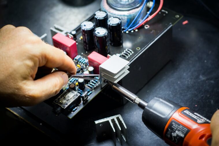
A printed circuit board, or PCB for short, is a base for various components that form patterns that can be used for different simple and complex projects. This structure is filled with layers with conductive and insulating traits. Their use is to provide a foundational building block for electronic devices across different industries and fields.
To get over the steps that are included in the design of PCB, we have to start with the electrical parameters. Specifically, we need to understand how the electrical parameters work. The electrical parameters include current maximums, voltages, signal types, capacitance limitations, impedance characteristics, shielding considerations, type and location of circuit components, and connectors.
Current maximums calculate the input current by using a couple of basic parameters and math integral to the field of electro engineering. It’s a rather simple process but the parameter itself is rather important.
Knowing the voltages on the electrical circuit is another necessary parameter. Their meaning is one of pressure from the electrical current’s power. The parameter of signal types is important to know in order to be able to read what’s being displayed or circulated throughout the board.
Impedance is in a similar spot as voltage as it dictates the measure of the opposition to the electrical flow within the circuit. Knowing this will help you better regulate the electrical flow. Of course, the capacity of electrical power itself is an important factor which is why capacitance limits are one of the other important parameters to get knowledgeable about.
Next up, you’ll need to shield all the components in order to keep them safe from potential interference. That’s a parameter we refer to as shielding considerations.
Lastly, you need to know proper nomenclature and uses for the types of components and connectors available. Their schematics and positioning on the circuit should be part of your overall knowledge.
Schematic
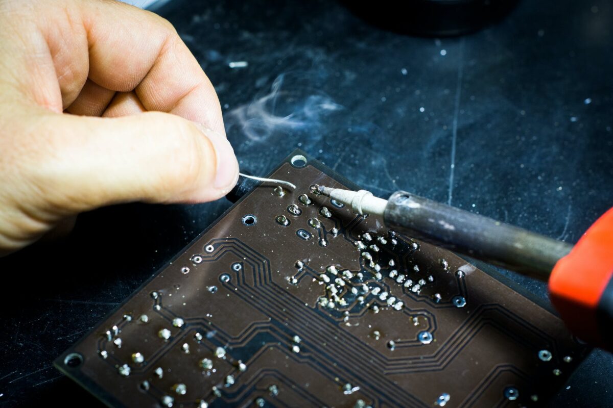
Once you have acquainted yourself with important parameters and become a bit more knowledgeable about the PCB, you’ll have to work on the schematic itself. The schematic is supposed to represent the design of the board’s overall components. Its function should be laid out with the schematic itself. Of course, keep in mind that the schematic is a very early stage of PCB’s creation so expect it to affect future steps.
The PCB design and layout are nonetheless important to the following process. They are blueprints that we will use as a base for the rest of the project. If you don’t feel confident crafting a schematic, you can always look at some from professional PCB design companies. After all, the PCB design process can be difficult for newbies to get a hang of and with the number of moving parts some people may wish to get some help into the whole process.
The layout of your PCB can be represented through a capture tool too. Using software that assists in PCB design presentation is a sure way of improving the quality of your PCB. Visit pcbasic.com to find out more about this.
Decide how much electricity can travel down a trace
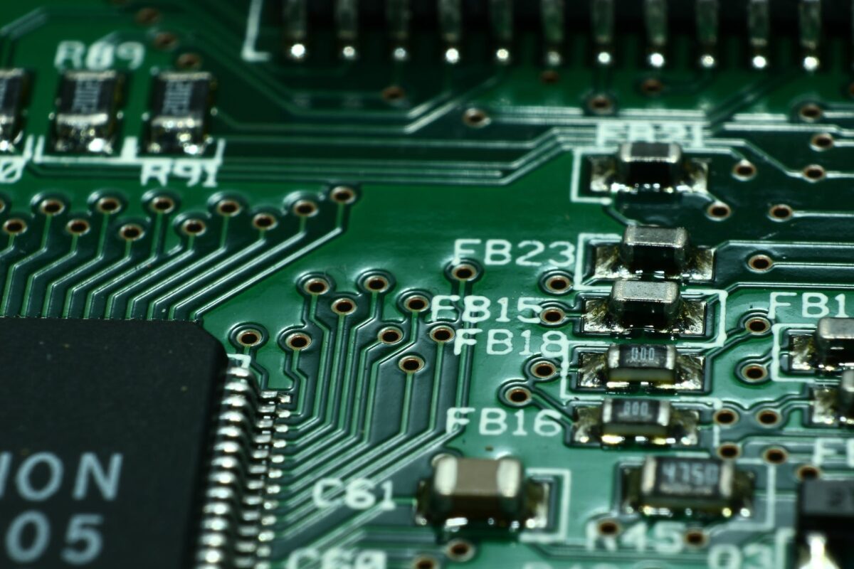
One of the things to consider when actually getting down to making a PCB design is to dictate how much electricity can travel down a trace at once. The importance of this task is one of the limits. If we know how much electricity we can get going through a trace and the circuit overall, we can better decide the functionality of components tied to the actual PCB.
It’s best to do this as early in the design as possible, if you do it later you may have to return and change some things around. While it could be a bit of a hassle the alternative is enduring malfunctions or potentially having the whole circuit not work.
Determine rules and requirements
While a PCB has its own design bits to consider, it should also conform to certain rules and requirements. The conditions and criteria are most frequently tied to IPC, which is the global association for electronics manufacturing. Their recommendations obviously carry a certain amount of weight.
The standards are to be understood before being applied, as their wrong usage could result in plentiful issues. Get deeply acquainted through available information before committing further. If you do proceed without proper preparation, you could end up struggling to fit the design pieces together.
Get to building the PCB

We are getting to the actual physical part now. In this step, you will place the components of the PCB according to the placement dictated by the design. Even as early as this step we see the importance of knowing standards. That’s because certain standards could dictate whether a component can be placed near another or whether it can be placed in some places at all.
There are a lot of complex interactions between components that you can’t quite get without knowing standards properly. If you do, then this should be easy enough. Simply place components in their respective areas and see if there’s anything amiss.
Get connections done
During this step, you’ll achieve connections between the layers inside of the circuit and get them interacting. This again beckons knowledge of standards but it also utilizes a lot of your design features that would have been done a few steps back. Don’t worry about taking extra time in this department, proper connections make sure everything is working as intended.
A part of achieving connections is also routing the tracers. This will connect segments to the electrical path that delivers electrical flow to the components. That way you’ll get to dictate what gets turned on when and whether they get to act at all.
Make your PCB readable
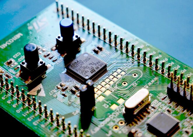
Once you’ve finished the more mechanical parts of the business. It’s time to make the PCB more readable for anybody but us. It’s a given that we’ll understand most of the interactions and components present but somebody just getting the circuit may not be as acquainted with the components used. It’s also just better if components are immediately labeled so that the person can get a hang of the entire flow of the circuit easier. To do so, name and label every item possible. Use marks and designators to make sure everything is properly located and information gets brought over quickly.
Generate PCB files
The last step is to get the layout into a file. Once we’ve turned them into a proper file format, the printed circuit board will be ready for production. The files will contain any important information and most of the design will be apparent from the contents of these files. Now get ready to make some printed circuit boards with the steps above.


